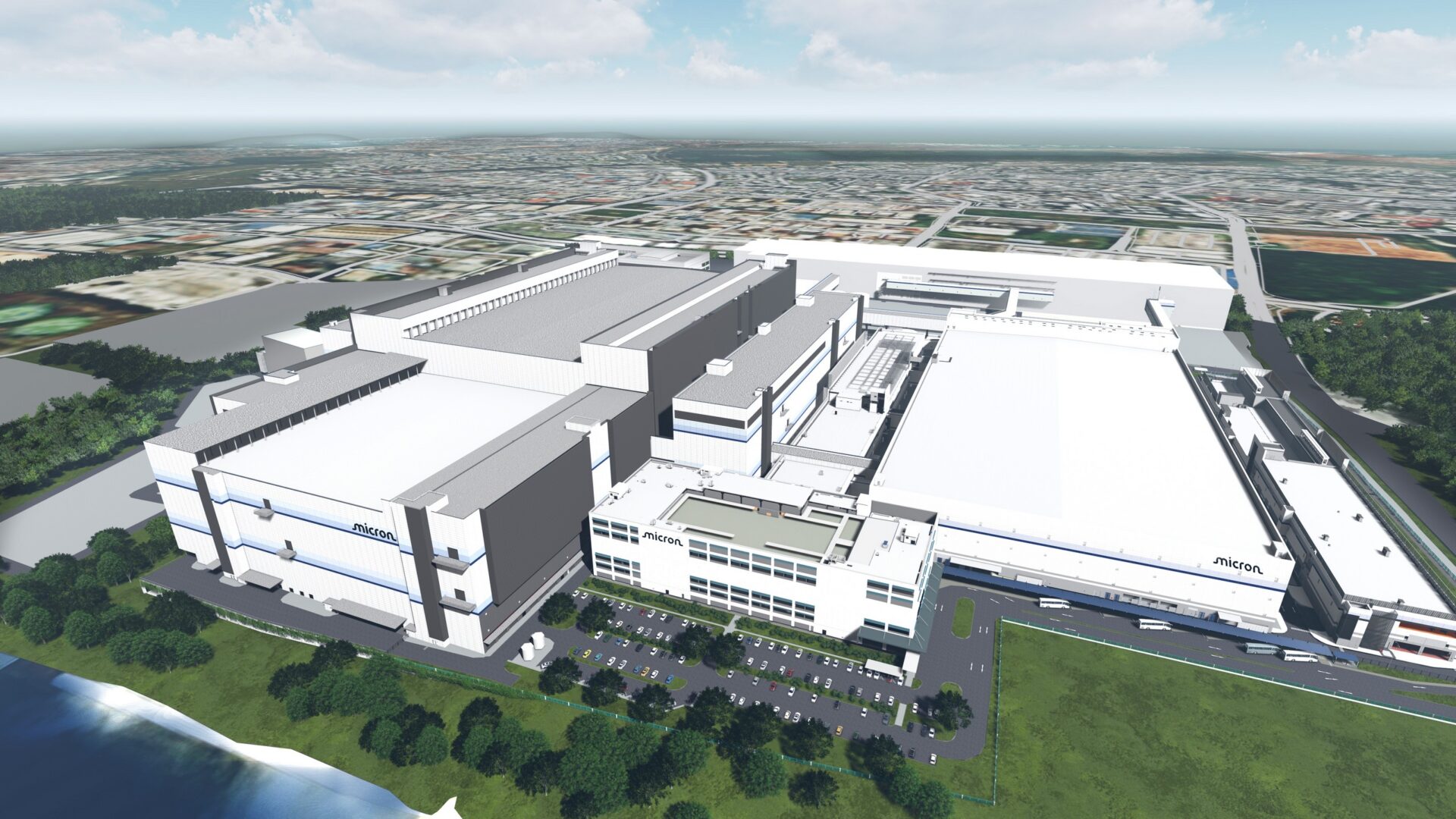
Micron Technology is investing US$7 billion in a cutting-edge semiconductor packaging facility in Woodlands, in northern Singapore, that will help manufacture the high-bandwidth memory (HBM) chips in high demand for AI applications today.
With operations to kick off in 2026, the facility will focus on HBM packaging operations. HBM technology is the stacking of memory chips for blazing speed, higher capacity, and lower power use and is the backbone of AI accelerators and data centres.
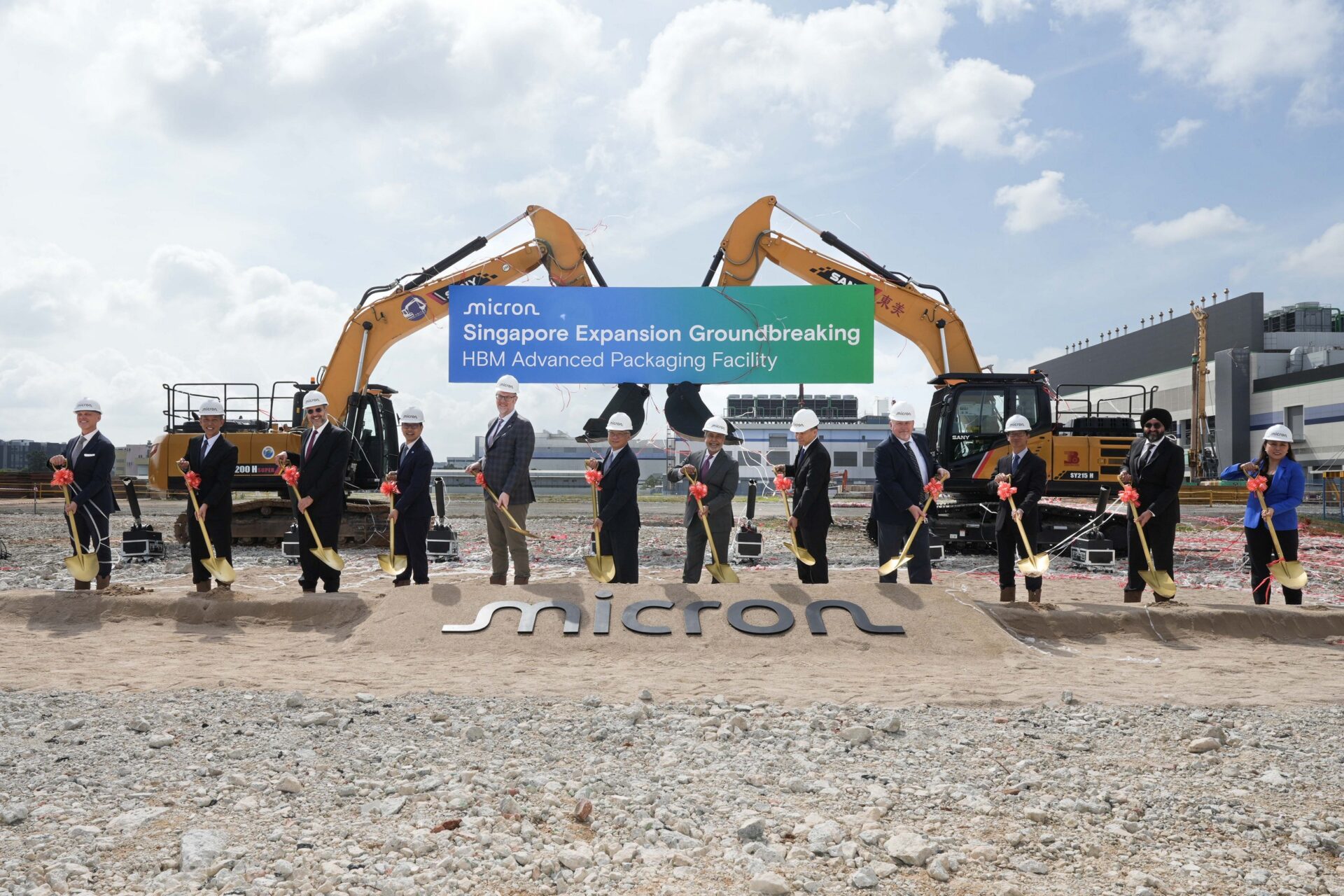
The market is exploding in line with the boom in AI. “We’re looking at HBM growth from US$4 billion in 2023 to over US$100 billion by 2030,” said Micron’s CEO Sanjay Mehrotra at the groundbreaking ceremony on January 8. “That’s bigger than today’s entire DRAM market.”
With demand for AI surging, the need for memory and storage has never been more critical, he said, adding that HBM will play an ever-growing role in the value proposition of AI accelerators, where HBM silicon holds a 7-to-1 ratio in terms of performance per area.
There are many reasons for HBM’s increasing importance. The key is its higher data transfer rates, which are crucial for heavy AI workloads that require massive amounts of data processing in real time. HBM is also a staple in GPUs, enabling seamless rendering for gaming, augmented reality/virtual reality, and simulation applications.
HBM’s ability to handle large datasets with low latency makes it indispensable for training large AI models and powering AI accelerators and inference engines.
Its compact design saves space on chips and allows integration with processors like GPUs and CPUs in tight form factors which is ideal for modern devices.
Micron’s new facility in Singapore, its latest investment in Singapore, will initially create 1,400 jobs, with plans to scale to 3,000 positions as the site expands in 2027. It will also enhance the Republic’s role in the global semiconductor supply chain.
A green facility, the new plant will feature greenhouse gas abatement systems, water recycling, and AI-powered automation, all aiming for LEED certification which means it is better for the environment, use fewer resources, and create less waste.
Globally, there is heightened interest in HBM. Key production and packaging facilities are clustered in regions with strong semiconductor ecosystems, including South Korea, Taiwan, the United States, and Singapore, with growing interest in China and Europe.
Singapore is a key node in the global semiconductor industry, accounting for one in 10 chips and one in five pieces of semiconductor equipment produced globally. In the past two years, Singapore has attracted S$18 billion in R&D and manufacturing investments.

Singapore’s Deputy Prime Minister, Gan Kim Yong, who was present at the groundbreaking ceremony, hailed the facility as a milestone for Singapore’s economy, placing the nation at the heart of the global AI and semiconductor boom.
“Micron’s investment cements our position as a critical player in the fast-growing AI space and strengthens our innovation-led economy,” he said.


